Central processing unit (CPU)
An Intel 80486DX2 CPU from above
An Intel 80486DX2 from below
The central processing unit (CPU) is the portion of a computer system that carries out the instructions of a computer program, to perform the basic arithmetical, logical, and input/output operations of the system. The CPU plays a role somewhat analogous to the brain in the computer. The term has been in use in the computer industry at least since the early 1960s.[1] The form, design and implementation of CPUs have changed dramatically since the earliest examples, but their fundamental operation remains much the same.
On large machines, CPUs require one or more printed circuit boards. On personal computers and small workstations, the CPU is housed in a single silicon chip called a microprocessor. Since the 1970s the microprocessor class of CPUs has almost completely overtaken all other CPU implementations. Modern CPUs are large scale integrated circuits in packages typically less than four centimeters square, with hundreds of connecting pins.
Two typical components of a CPU are the arithmetic logic unit (ALU), which performs arithmetic and logical operations, and the control unit (CU), which extracts instructions from memory and decodes and executes them, calling on the ALU when necessary.
Not all computational systems rely on a central processing unit. An array processor or vector processor has multiple parallel computing elements, with no one unit considered the "center". In the distributed computing model, problems are solved by a distributed interconnected set of processors.
The control unit
The control unit of the CPU contains circuitry that uses electrical signals to direct the entire computer system to carry out stored program instructions. The control unit does not execute program instructions; rather, it directs other parts of the system to do so. The control unit must communicate with both the arithmetic/logic unit and memory.
The design complexity of CPUs increased as various technologies facilitated building smaller and more reliable electronic devices. The first such improvement came with the advent of the transistor. Transistorized CPUs during the 1950s and 1960s no longer had to be built out of bulky, unreliable, and fragile switching elements like vacuum tubes and electrical relays. With this improvement more complex and reliable CPUs were built onto one or several printed circuit boards containing discrete (individual) components.
During this period, a method of manufacturing many transistors in a compact space gained popularity. The integrated circuit (IC) allowed a large number of transistors to be manufactured on a single semiconductor-based die, or "chip." At first only very basic non-specialized digital circuits such as NOR gates were miniaturized into ICs. CPUs based upon these "building block" ICs are generally referred to as "small-scale integration" (SSI) devices. SSI ICs, such as the ones used in the Apollo guidance computer, usually contained up to a few score transistors. To build an entire CPU out of SSI ICs required thousands of individual chips, but still consumed much less space and power than earlier discrete transistor designs. As microelectronic technology advanced, an increasing number of transistors were placed on ICs, thus decreasing the quantity of individual ICs needed for a complete CPU. MSI and LSI (medium- and large-scale integration) ICs increased transistor counts to hundreds, and then thousands.
In 1964 IBM introduced its System/360 computer architecture which was used in a series of computers that could run the same programs with different speed and performance. This was significant at a time when most electronic computers were incompatible with one another, even those made by the same manufacturer. To facilitate this improvement, IBM utilized the concept of a microprogram (often called "microcode"), which still sees widespread usage in modern CPUs.[3] The System/360 architecture was so popular that it dominated the mainframe computer market for decades and left a legacy that is still continued by similar modern computers like the IBM zSeries. In the same year (1964), Digital Equipment Corporation (DEC) introduced another influential computer aimed at the scientific and research markets, the PDP-8. DEC would later introduce the extremely popular PDP-11 line that originally was built with SSI ICs but was eventually implemented with LSI components once these became practical. In stark contrast with its SSI and MSI predecessors, the first LSI implementation of the PDP-11 contained a CPU composed of only four LSI integrated circuits.[4]
Transistor-based computers had several distinct advantages over their predecessors. Aside from facilitating increased reliability and lower power consumption, transistors also allowed CPUs to operate at much higher speeds because of the short switching time of a transistor in comparison to a tube or relay. Thanks to both the increased reliability as well as the dramatically increased speed of the switching elements (which were almost exclusively transistors by this time), CPU clock rates in the tens of megahertz were obtained during this period. Additionally while discrete transistor and IC CPUs were in heavy usage, new high-performance designs like SIMD (Single Instruction Multiple Data) vector processors began to appear. These early experimental designs later gave rise to the era of specialized supercomputers like those made by Cray Inc.
Microprocessors
the 1970s the fundamental inventions by Federico Faggin (Silicon Gate MOS ICs with self aligned gates along with his new random logic design methodology) changed the design and implementation of CPUs forever. Since the introduction of the first commercially available microprocessor (the Intel 4004), in 1970 and the first widely used microprocessor (the Intel 8080) in 1974, this class of CPUs has almost completely overtaken all other central processing unit implementation methods. Mainframe and minicomputer manufacturers of the time launched proprietary IC development programs to upgrade their older computer architectures, and eventually produced instruction set compatible microprocessors that were backward-compatible with their older hardware and software. Combined with the advent and eventual vast success of the now ubiquitous personal computer, the term CPU is now applied almost exclusively to microprocessors. Several CPUs can be combined in a single processing chip.
Previous generations of CPUs were implemented as discrete components and numerous small integrated circuits (ICs) on one or more circuit boards. Microprocessors, on the other hand, are CPUs manufactured on a very small number of ICs; usually just one. The overall smaller CPU size as a result of being implemented on a single die means faster switching time because of physical factors like decreased gate parasitic capacitance. This has allowed synchronous microprocessors to have clock rates ranging from tens of megahertz to several gigahertz. Additionally, as the ability to construct exceedingly small transistors on an IC has increased, the complexity and number of transistors in a single CPU has increased dramatically. This widely observed trend is described by Moores law, which has proven to be a fairly accurate predictor of the growth of CPU (and other IC) complexity to date.
While the complexity, size, construction, and general form of CPUs have changed drastically over the past sixty years, it is notable that the basic design and function has not changed much at all. Almost all common CPUs today can be very accurately described as von Neumann stored-program machines. As the aforementioned Moores law continues to hold true, concerns have arisen about the limits of integrated circuit transistor technology. Extreme miniaturization of electronic gates is causing the effects of phenomena like electromigration and subthreshold leakage to become much more significant. These newer concerns are among the many factors causing researchers to investigate new methods of computing such as the quantum computer, as well as to expand the usage of parallelism and other methods that extend the usefulness of the classical von Neumann model.
The fundamental operation of most CPUs, regardless of the physical form they take, is to execute a sequence of stored instructions called a program. The program is represented by a series of numbers that are kept in some kind of computer memory. There are four steps that nearly all CPUs use in their operation: fetch, decode, execute, and writeback.
The first step, fetch, involves retrieving an instruction (which is represented by a number or sequence of numbers) from program memory. The location in program memory is determined by a program counter (PC), which stores a number that identifies the current position in the program. After an instruction is fetched, the PC is incremented by the length of the instruction word in terms of memory units.[5] Often, the instruction to be fetched must be retrieved from relatively slow memory, causing the CPU to stall while waiting for the instruction to be returned. This issue is largely addressed in modern processors by caches and pipeline architectures (see below).
The instruction that the CPU fetches from memory is used to determine what the CPU is to do. In the decode step, the instruction is broken up into parts that have significance to other portions of the CPU. The way in which the numerical instruction value is interpreted is defined by the CPUs instruction set architecture (ISA).[6] Often, one group of numbers in the instruction, called the opcode, indicates which operation to perform. The remaining parts of the number usually provide information required for that instruction, such as operands for an addition operation. Such operands may be given as a constant value (called an immediate value), or as a place to locate a value: a register or a memory address, as determined by some addressing mode. In older designs the portions of the CPU responsible for instruction decoding were unchangeable hardware devices. However, in more abstract and complicated CPUs and ISAs, a microprogram is often used to assist in translating instructions into various configuration signals for the CPU. This microprogram is sometimes rewritable so that it can be modified to change the way the CPU decodes instructions even after it has been manufactured.
After the fetch and decode steps, the execute step is performed. During this step, various portions of the CPU are connected so they can perform the desired operation. If, for instance, an addition operation was requested, the arithmetic logic unit (ALU) will be connected to a set of inputs and a set of outputs. The inputs provide the numbers to be added, and the outputs will contain the final sum. The ALU contains the circuitry to perform simple arithmetic and logical operations on the inputs (like addition and bitwise operations). If the addition operation produces a result too large for the CPU to handle, an arithmetic overflow flag in a flags register may also be set.
The final step, writeback, simply "writes back" the results of the execute step to some form of memory. Very often the results are written to some internal CPU register for quick access by subsequent instructions. In other cases results may be written to slower, but cheaper and larger, main memory. Some types of instructions manipulate the program counter rather than directly produce result data. These are generally called "jumps" and facilitate behavior like loops, conditional program execution (through the use of a conditional jump), and functions in programs.[7] Many instructions will also change the state of digits in a "flags" register. These flags can be used to influence how a program behaves, since they often indicate the outcome of various operations. For example, one type of "compare" instruction considers two values and sets a number in the flags register according to which one is greater. This flag could then be used by a later jump instruction to determine program flow.
واحد پردازش مرکزی (CPU)
بخشی از یک سیستم کامپیوتری است که انجام دستورالعمل از یک برنامه کامپیوتری ، به انجام عملیات پایه محاسباتی ، منطقی ، و ورودی / خروجی از سیستم می باشد. CPU نقش تا حدودی شبیه به مغز در کامپیوتر است. این اصطلاح در حال استفاده در صنعت رایانه حداقل از سال 1960s اولیه بوده است. [1] فرم ، طراحی و پیاده سازی پردازنده به طرز چشمگیری از اولین نمونه های تغییر است ، اما عملیات اساسی خود باقی می ماند بسیار مشابه است.
پردازنده بر روی ماشین های بزرگ ، نیاز به یک یا چند تخته مدار چاپ شده است. بر روی کامپیوترهای شخصی و ایستگاه های کاری کوچک ، CPU در یک چیپ سیلیکونی مجزا به نام ریز پردازنده قرار دارد. از 1970s کلاس ریز پردازنده پردازنده ها تقریبا به طور کامل پیشی گیرد و تمام پیاده سازی های CPU های دیگر است. پردازنده های مدرن مدارهای مجتمع در مقیاس بزرگ در بسته های به طور معمول کمتر از چهار سانتی متر مربع ، با صدها نفر از پین های اتصال است.
دو مولفه نوعی از CPU ، واحد حساب و منطق (ALU) ، که به انجام عملیات حسابی و منطقی و واحد کنترل (CU) ، عصاره است که دستورالعمل ها را از حافظه و رمزگشائی و جوخه اعدام می سپارد ، با دعوت از ALU در صورت لزوم.
در یک واحد پردازش مرکزی سیستم های محاسباتی تکیه می کنند. پردازنده آرایه یا بردار پردازنده دارای عناصر متعدد محاسبات موازی ، بدون واحد در نظر گرفته "مرکز" است. در مدل محاسبات توزیع شده ، مشکلات توسط یک مجموعه به هم پیوسته توزیع پردازنده حل شده است.
واحد کنترل
واحد کنترل CPU شامل مدارات استفاده می کند که سیگنال های الکتریکی را به مستقیم از کل سیستم کامپیوتری به انجام دستورالعمل های ذخیره شده برنامه. واحد کنترل به دستورالعمل برنامه را اجرا نیست ، بلکه بر آن هدایت بخش های دیگر این سیستم را به انجام این کار. واحد کنترل باید با هر دو واحد ریاضی / منطق و حافظه ارتباط برقرار کند.
ترانزیستور گسسته و مدار مجتمع پردازنده
پیچیدگی طراحی پردازنده ها افزایش یافته و به عنوان فن آوری های مختلف تسهیل ساخت دستگاه های کوچکتر و قابل اطمینان تر الکترونیکی. اولین بهبود از جمله با ظهور ترانزیستور آمد. پردازنده ترانزیستوری در طول 1950s و 1960s دیگر تا به حال به از عناصر حجیم ، غیر قابل اعتماد ، و شکننده سوئیچینگ مانند لامپ خلاء و رله های الکتریکی ساخته شده است. با استفاده از این بهبود ، پیچیده تر و قابل اعتماد پردازنده بر روی یک یا چندین تخته مدار چاپ شده که حاوی) قطعات گسسته (فردی ساخته شده بودند.
در طی این دوره ، روش ساخت بسیاری از ترانزیستور در یک فضای فشرده را به دست اورد محبوبیت. مدار مجتمع (IC) اجازه داد تا تعداد زیادی از ترانزیستورها بر روی نیمه هادی تک مبتنی بر می میرند ، یا تولید "چیپ". در ابتدا تنها مدارات غیر تخصصی پایه های دیجیتال مانند NOR دروازه به ICS کوچک شد. پردازنده مبتنی بر این "بلوک ساختمان" ICS به طور کلی به عنوان "مجتمع سازی در مقیاس کوچک (SSI) دستگاه می گویند. مدارات مجتمع SSI ، مانند آنهایی که در کامپیوتر هدایت آپولو مورد استفاده قرار ، معمولا حاوی تا چند ترانزیستور نمره. برای ساخت CPU کل مدارات مجتمع SSI مورد نیاز هزاران نفر از تراشه های فردی ، اما هنوز هم مصرف فضای بسیار کمتر و قدرت نسبت به ترانزیستور طرح زودتر گسسته. به عنوان علم میکرو الکترونیک و فن آوری پیشرفته ، افزایش تعداد ترانزیستورها در مدارات مجتمع قرار داده شد ، در نتیجه کاهش مقدار IC های فردی مورد نیاز برای یک پردازنده کامل. MSI و LSI (متوسط و مجتمع سازی در مقیاس بزرگ) ICS افزایش تعداد ترانزیستور را به صدها و پس از آن هزاران.
آی بی ام در سال 1964 معرفی معماری System/360 کامپیوتر خود را که در یک سری از رایانه هایی است که می تواند برنامه های مشابه با سرعت های مختلف و کارایی اجرا مورد استفاده قرار گرفت. این قابل توجهی در یک زمان بود که بیشتر کامپیوترهای الکترونیکی با یکدیگر ، حتی آنهایی که ساخته شده توسط کارخانه سازنده ناسازگار بودند. برای تسهیل این بهبود ، آی بی ام با بهرهگیری از مفهوم ریز برنامه (که اغلب به نام "ریز") ، که هنوز هم استفاده گسترده در CPU های مدرن می بیند. [3] معماری System/360 چنان محبوب بود که آن را بازار کامپیوتر های پردازنده مرکزی برای چند دهه تحت سلطه و سمت چپ میراثی است که هنوز هم توسط کامپیوترهای مدرن مشابه مانند IBM zSeries ادامه داد. شرکت تجهیزات دیجیتال (دسامبر) در همان سال (1964) ، معرفی یک کامپیوتر دیگر و با نفوذ با هدف در بازارهای علمی و پژوهشی ، PDP - 8. دسامبر بعدها بسیار محبوب PDP - 11 خط است که در اصل با مدارات مجتمع SSI ساخته شده بود ، اما نهایتا با اجزاء LSI اجرا شد پس از این شد عملی معرفی نماید. در تضاد کامل با SSI و MSI پیشینیان ، اولین پیاده سازی LSI از PDP - 11 شامل یک پردازنده متشکل از تنها چهار LSI مدار مجتمع است. [4]
رایانه مبتنی بر ترانزیستور به حال چندین مزیت متمایز بیش از پیشینیان خود است. گذشته از تسهیل قابلیت اطمینان افزایش یافته و مصرف انرژی کمتر ، ترانزیستورها نیز مجاز CPU ها در سرعت های بسیار بالاتر به علت زمان سوئیچینگ کوتاه یک ترانزیستور در مقایسه با یک لوله و یا رله عمل است. با تشکر از هر دو افزایش قابلیت اطمینان و همچنین افزایش سرعت به طرز چشمگیری از عناصر سوئیچینگ (که تقریبا به طور انحصاری ترانزیستور در این زمان) ، نرخ کلاک پردازنده در ده ها مگاهرتز در طول این مدت به دست آمد. به علاوه در حالی که ترانزیستور گسسته و IC CPU ها در استفاده های سنگین ، طرح های جدید با عملکرد بالا مانند SIMD (آموزش اطلاعات تنها چندگانه) پردازنده بردار شروع به نظر می رسد. این طرح اوایل تجربی بعد باعث به عصر تخصصی ابر رایانه ها مانند آنهایی که ساخته شده توسط شرکت Cray
ریزپردازنده
1970s اختراعات بنیادی که توسط Federico Faggin (MOS IC های سیلیکون دروازه با دروازه های خود تراز وسط قرار دارد همراه با منطق تصادفی جدید خود را به روش های طراحی) طراحی و پیاده سازی پردازنده ها را برای همیشه تغییر است. از آنجا که مقدمه ، نخستین ریزپردازنده تجاری در دسترس (اینتل 4004) در سال 1970 و به طور گسترده استفاده می شود اولین ریزپردازنده (اینتل | 8080) در سال 1974 ، این کلاس از پردازنده ها تقریبا به طور کامل با پیشی گیرد و تمام دیگر روشهای پیاده سازی واحد پردازش مرکزی است. سازندگان مینی کامپیوتر های پردازنده مرکزی و از زمان راه اندازی برنامه های توسعه IC اختصاصی به روز رسانی معماری کامپیوتر های قدیمی تر خود را ، و دستور العمل در نهایت تولید ریزپردازنده های سازگار که عقب مانده سازگار با خود را سخت افزار و نرم افزار های قدیمی تر بودند. همراه با ظهور و موفقیت احتمالی قریب به اتفاق از کامپیوتر شخصی در حال حاضر در همه جا ، CPU مدت در حال حاضر تقریبا به طور انحصاری به ریزپردازنده استفاده شود. پردازنده های متعددی می تواند در یک تراشه واحد پردازش ترکیب شده است.
نسل قبلی پردازنده ها به عنوان اجزای گسسته و متعدد کوچک از مدارهای یکپارچه (ICS) یک یا بیشتر بر روی تخته مدار به اجرا در آمد. ریزپردازنده ، از سوی دیگر ، پردازنده ها در تعداد بسیار کمی از ICS تولید ، معمولا فقط یکی است. به طور کلی اندازه کوچک تر CPU به عنوان یک نتیجه که در جان تک اجرا به این معنی سریعتر زمان سوئیچینگ به دلیل عوامل فیزیکی مانند کاهش ظرفیت خازنی گیت انگلی. این اجازه داده است ریزپردازنده همزمان به نرخ های ساعت گرفته تا ده ها مگاهرتز به گیگاهرتز چند. علاوه بر این ، به عنوان توانایی ساخت ترانزیستورهای بسیار کوچک بر روی یک IC افزایش یافته است ، پیچیدگی و تعداد ترانزیستورها در یک پردازنده واحد افزایش یافته است به طور چشمگیری است. این روند به طور گسترده ای مشاهده می شود توسط قانون مور ، که ثابت کرده است که یک پیش بینی نسبتا دقیق از رشد پیچیدگی CPU (و دیگر IC) تا به امروز توصیف کرد.
در حالیکه پیچیدگی ، اندازه ، ساخت و ساز ، و به شکل کلی پردازنده ها در طول شصت سال گذشته به شدت تغییر کرده ، این نکته قابل توجهاست که طراحی اولیه و عملکرد در همه تغییر نکرده است. امروز تقریبا تمام CPU های مشترک می تواند بسیار دقیق به عنوان برنامه ذخیره ماشین آلات فون نویمان شرح داده شده است. به عنوان فوق الذکر قانون مور همچنان برای برگزاری درست ، نگرانی در مورد محدودیت های ترانزیستور از تکنولوژی مدار مجتمع بوجود آمده اند. کوچک سازی افراطی از دروازه الکترونیکی است باعث اثرات پدیده های مانند electromigration و نشت subthreshold برای تبدیل شدن به بسیار مهمتر است. این نگرانی های جدیدتر در میان عوامل بسیاری باعث محققان به بررسی روش های جدید محاسباتی مانند کامپیوتر کوانتومی ، و همچنین به گسترش استفاده از موازی سازی و روش های دیگر که گسترش سودمندی مدل کلاسیک فون نویمان هستند.
عمل
عملیات اساسی اکثر ریزپردازنده ها ، بدون در نظر گرفتن شکل فیزیکی آنها را ، این است که اجرای دنباله ای از دستورالعمل های ذخیره شده به نام یک برنامه است. برنامه توسط یک سری از اعداد است که در نوعی از حافظه کامپیوتر نگهداری می شود نشان داده شده است. چهار مرحله که تقریبا تمام سی پی یو در عملیات خود استفاده وجود دارد : واکشی ، رمزگشایی ، اجرا و writeback.
گام اول ، واکشی ، شامل بازیابی دستورالعمل (که توسط یک عدد یا دنباله ای از اعداد نشان داده شده است) را از حافظه برنامه. محل در حافظه برنامه توسط شمارنده برنامه (PC) است که فروشگاه ها یک تعداد مشخص است که موقعیت فعلی را در برنامه تعیین می شود. بعد از آموزش از ذهن است ، PC توسط طول کلمه دستورالعمل در واحد حافظه واحد اضافه شده است. [5] اغلب ، دستور به دستور ذهن باید از حافظه نسبتا آهسته بازیابی CPU که این کار را می کند ، و باعث به غرفه حالی که در انتظار دستور به دستور برگردانده می شود. این مسئله تا حد زیادی که در پردازنده های مدرن توسط انبارها و معماری خط لوله (پایین را ببینید) خطاب شده است.
دستور العمل است که پردازنده از حافظه واکشی می باشد استفاده می شود برای تعیین آنچه CPU برای انجام شده است. در مرحله رمزگشایی ، دستورالعمل به بخش های است که دارای اهمیت به بخش های دیگر از CPU شکسته شده است. روشی که در آن دستور مقدار عددی است به تفسیر توسط پردازنده معماری مجموعه دستورالعمل (ISA) تعریف شده است. [6] اغلب ، یک گروه از اعداد در آموزش ، opcode نامیده می شود ، نشان می دهد که عملیات به انجام است. قطعات باقی مانده از شماره معمولا اطلاعات مورد نیاز برای آن دستور ، مانند عملوندهای برای عملیات علاوه بر ارائه می کنند. عملوندهای چنین ممکن است به عنوان یک مقدار ثابت (به نام ارزش فوری) داده می شود یا به عنوان یک مکان برای قرار دادن ارزش : ثبت نام و یا آدرس حافظه که توسط برخی از حالت پرداختن به تعیین. در طراحی های قدیمی تر بخشی از CPU مسئول رمز گشایی برای آموزش دستگاه های سخت افزاری غیر قابل تغییر شد. با این حال ، در پردازنده های انتزاعی تر و پیچیده تر و ISAS ، حافظه است که اغلب مورد استفاده قرار گیرد به کمک در ترجمه دستورالعمل ها را به سیگنال های مختلف تنظیمات برای CPU است. این ریز برنامه گاهی قابلیت دوباره نویسی شده است به طوری که می توان آن را اصلاح برای تغییر راه CPU دستورالعمل رمزگشائی حتی پس از آن تولید شده است.
پس از واکشی و رمزگشایی مراحل ، مرحله اجرا است انجام می شود. در طول این مرحله ، بخش های مختلف از CPU متصل هستند به طوری که آنها می توانید عملیات مورد نظر انجام است. اگر ، برای مثال ، عملیات علاوه بر درخواست شده بود ، واحد حساب و منطق (ALU) به مجموعه ای از نهاده ها و مجموعه ای از خروجی متصل خواهد شد. ورودی های ارائه شماره به آن اضافه شود ، و خروجی حاصل جمع نهایی باشد. ALU شامل مدارات به انجام حساب ساده و عملیات منطقی بر روی ورودی (مانند علاوه بر این و عملیات بیتی). اگر این عملیات علاوه بر تولید بیش از حد بزرگ برای پردازنده که مسئولیت رسیدگی به نتیجه ، حسابی پرچم سرریز در یک ثبات پرچم نیز ممکن است مجموعه ای می شود.
گام نهایی ، writeback ، به سادگی "می نویسد :" از پشت به نتایج مرحله اجرا به نوعی از حافظه است. خیلی اوقات نتایج به دست آمده به برخی از ثبت نام CPU داخلی برای دسترسی سریع دستورالعمل های بعدی نوشته شده است. در موارد دیگر ممکن است کندتر است ، اما ارزان تر و بزرگتر است ، حافظه اصلی نوشته شده است. برخی از انواع از دستورالعمل دستکاری شمارنده برنامه نه به طور مستقیم تولید داده نتیجه. این ها عموما به نام «جهش» و تسهیل رفتار مانند حلقه ها ، اجرای برنامه های مشروط (از طریق استفاده از جهش شرطی) ، و توابع در برنامه است. [7] دستورالعمل بسیاری نیز تغییر خواهد کرد دولت از رقم در "پرچم" ثبت نام کنید. این پرچم را می توان مورد استفاده برای نفوذ در نحوه رفتار یک برنامه ، از آنجایی که آنها اغلب نتیجه عملیات های مختلف نشان می دهد. به عنوان مثال ، یک نوع "مقایسه" را دستور العمل به این دو ارزش ها و مجموعه تعداد در پرچم های نصب شده ثبت نام با توجه به که کدام یک بزرگتر است. این پرچم را می توان توسط یک دستور پرش بعدی برای تعیین جریان برنامه مورد استفاده قرار گیرد.
سایت: www.daneshyaran.4kia.ir
 دانلود طرح لایه باز اعلامیه ترحیم (11) (دانش یاران)
 دانلود پک کامل کادر دور صفحه برگرفته از تمامی طرح های متنوع (دانش یاران)
 نمونه اجاره نامه مسکونی تجاری همراه با اصل فایل(دانش یاران)
 دانلود پک کامل طرح های حاشیه گوشه و کنار صفحه با کیفیت بالا (دانش یاران )
 دانلود طرح لایه باز تقدیر نامه و لوح سپاس(18)( دانش یاران)
 نمونه دعوت نامه هفته دفاع مقدس (دانش یاران)
 دانلود طرح لایه باز تقدیرنامه(12)( دانش یاران)
 دانلود طرح لایه باز فاکتور فروشگاه لوازم خانگی(دانش یاران)(2)
 دانلود طرح لایه باز تقدیر نامه و لوح سپاس(17)(دانش یاران)
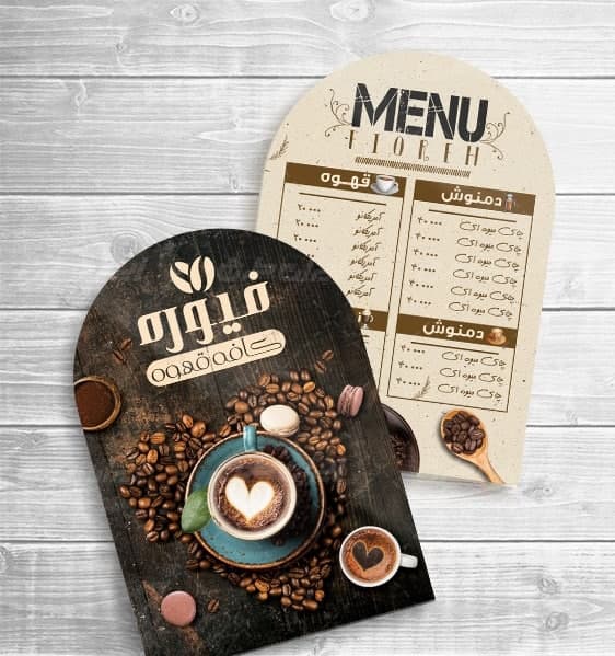 دانلود طرح لایه باز منو کافه، قهوه خانه ، ساندویچی، تهیه غذا (4))(دانش یاران )
 طرح اعلامیه و بنر های هیئت های مذهبی (دانش یاران)
 طرح اعلامیه و بنر های هیئت های مذهبی(دانش یاران)
 طرح اعلامیه و بنر های هیئت های مذهبی(دانش یاران)
 اثر آگاهی از نتایج بر عملکرد (دانش یاران)
 گزارش تخصصی پایه ابتدایی با عنوان حل مشکل بدخطی و نارسانویسی یکی از دانش آموزان (دانش یاران)
 طرح اعلامیه و بنر های هیئت های مذهبی (دانش یاران)
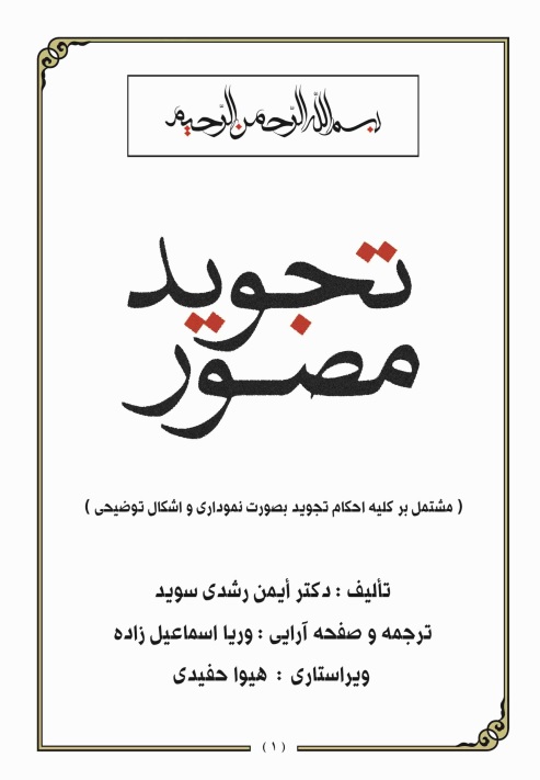 دانلود رایگان کتاب تجوید مصور نوشته دکتر ایمن رشدی سوید با لینک مستقیم (دانش یاران)
 تحقیق در مورد آب (دانش یاران)
 دانلود طرح لایه باز کارت ویزیت رایگان بیمه ایران (1)(دانش یاران)
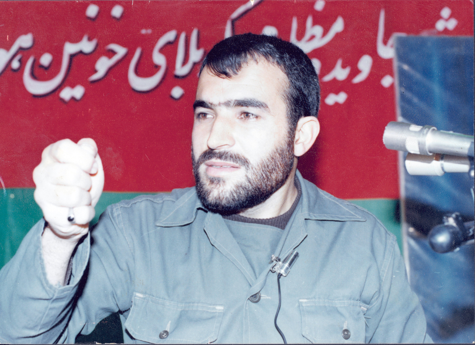 آلبوم تصاویر سردار شهید اسماعیل صادقی (دانش یاران) دانلود طرح لایه باز اعلامیه ترحیم (11) (دانش یاران) نمونه اجاره نامه مسکونی تجاری همراه با اصل فایل(دانش یاران) دانلود طرح لایه باز تقدیر نامه و لوح سپاس(18)( دانش یاران) نمونه دعوت نامه هفته دفاع مقدس (دانش یاران)
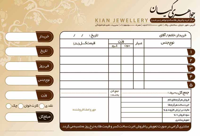 فاکتور فروش لایه باز وقابل تغییرات / طلا و جواهرات (دانش یاران) دانلود پک کامل کادر دور صفحه برگرفته از تمامی طرح های متنوع (دانش یاران) دانلود پک کامل طرح های حاشیه گوشه و کنار صفحه با کیفیت بالا (دانش یاران )
 دانلود طرح لایه باز تقدیر نامه (2) (دانش یاران) دانلود طرح لایه باز فاکتور فروشگاه لوازم خانگی(دانش یاران)(2) دانلود طرح لایه باز تقدیرنامه(12)( دانش یاران)
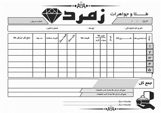 طرح لایه باز فاکتور فروش قابل تغییرات طلا و جواهرات (دانش یاران)
 دانلود طرح لایه باز بنر عرض تسلیت و فوت (6)(دانش یاران)